Developing market-specific thin-film technologies and deposition tools that improve our client's productivity
Proof of Concept
Test of layer / substrate performance and basic parameters at SolayerEvaluation & Validation
Process development and parameter optimization, both at Solayer and customer siteDesign & Development
Tool design, manufacturing and process optimization based on customer feedbackInstallation & Support
Final testing and transfer of process and production tool to customer site- Our capabilities and selected successful projects -

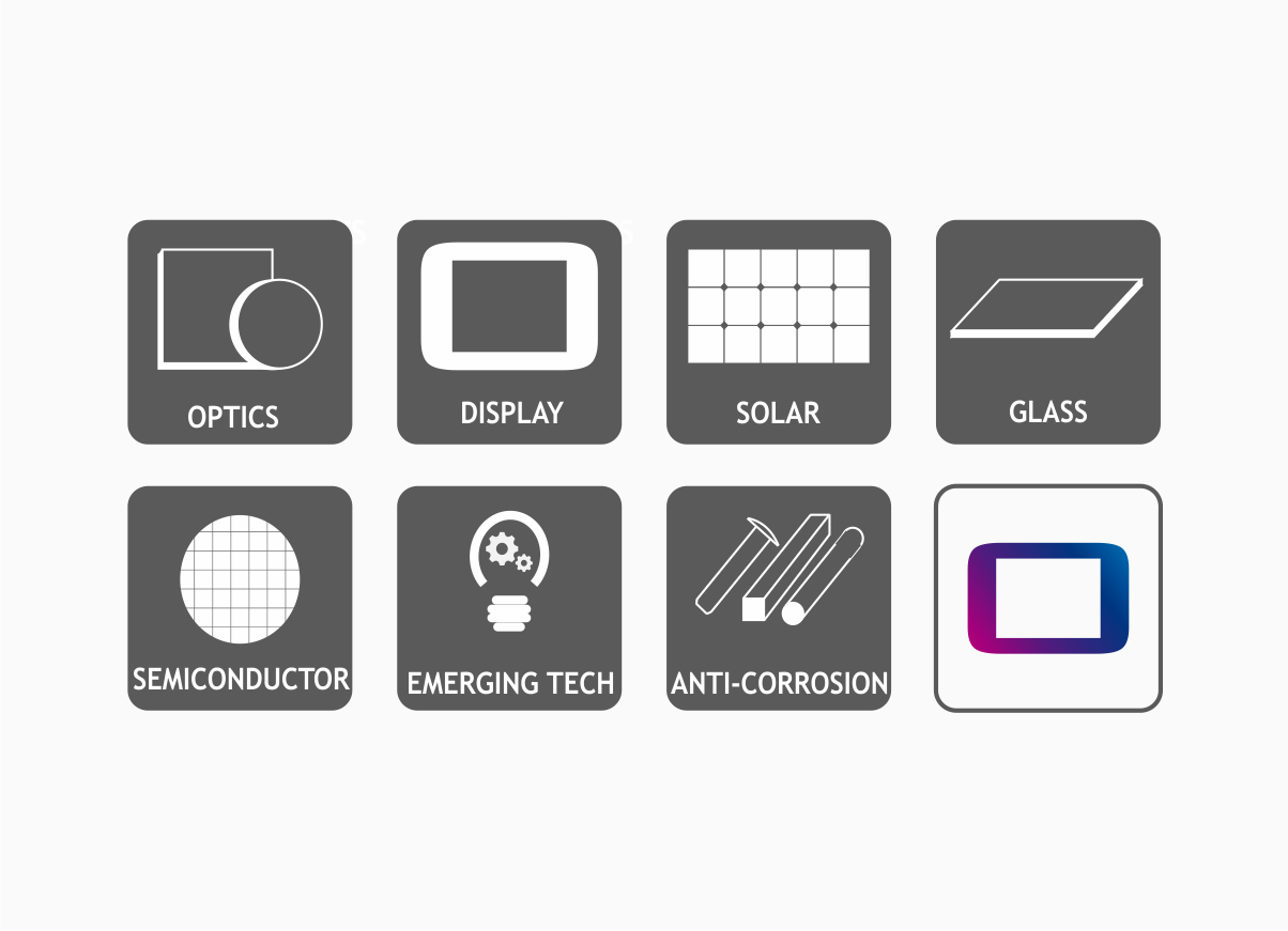
Technology Development:
- Coatings for optical filters, mirrors, lenses and other components ranging from a few layers up to 200+ layers.
Coating Tools:
- Unique sputter deposition tools designed especially for the precision optics market. Ranging from small size substrate like smartphone cover glass to large size mass production equipment as well as equipment for cutting-edge precision optics applications. The portfolio gives the customers a good market entry with minimal cost of ownership at very low CAPEX. Read more >>>

Technology Development:
- Sputtering of front & back contacts, functional interlayers and barrier layers for thin film photovoltaics.
Coating Tools:
- Inline deposition tools for anti-reflection and passivation layers based on magnetron sputtered SiON from rotatable cathodes and PECVD-based SiN.
- Versatile cluster tool for CIGS deposition that allows sputtering, evaporation, ALD, IBAD, PLD, FLA and analytics.

Technology Development:
- Advanced process to deposit ITO layers at less than 100ºC substrate temperature for display applications.
Process Components:
- Rotatable magnetron sputtering components consisting of magnet bars and end blocks for FPD application.
Surface Treatment:
- Integration of FLA modules into inline system to improve properties of TCO on temperature-sensitive substrates.

Technology Development:
- Anti-scratch decorative coating and low-E architectural glazing for rigid glass by PVD, PECVD and ion treatment.
Coating Tool:
- ALD tool to deposit ultra-thin Tungsten layers inside glass capillary tubes for medical X-ray applications.
Surface Treatment:
- FLA treatment of large-area TCO thin film on thin glass and other flexible substrates.

Technology Development:
- Dopant activation and recrystallization of Si, Ge, SiC, GaAs, GaN, InP etc. by Flash Lamp Annealing (FLA).
Coating Tools:
- A high-voltage ion implantation and deposition system at low cost of ownership for plasma doping in microelectronics.
- R & D Co-sputter cluster tool with advanced angle / T-S position adjustment and gradient / mixed layer deposition.

Technology Development:
- Evaporation of organic solvent and sintering of nano-particles in printed layers on glass, polymer, paper, textiles etc..
Coating Tools:
- Customized design and development of OLED deposition tool for display applications.
- Roll-to-Roll (R2R) equipment for sputtering and evaporation of ultra-thin metallic layers.

Technology Development:
- An economical low-temperature plasma process based on combined PVD / Evaporation for steel galvanization.
Coating Tools:
- Inline vacuum coating system of steel products - bars, beams, screws etc. - with high-quality zinc.
- Batch processing system for the deposition of hard and protective layers by plasma-based ion implantation.